Image source: The Motley Fool.
Atomera Inc (ATOM -1.24%)
Q1 2021 Earnings Call
Apr 28, 2021, 5:00 p.m. ET
Contents:
- Prepared Remarks
- Questions and Answers
- Call Participants
Prepared Remarks:
Mike Bishop
Hello, everyone, and welcome to Atomera's first-quarter fiscal year 2021 earnings webinar. I'd like to remind everyone that this call and webinar are being recorded, and a replay will be available on Atomera's IR website for one year. I'm Mike Bishop with the company's investor relations. After a positive experience last quarter, we are again using Zoom and we will follow a similar format to prior quarters with participants in a listen-only mode.
We will open with prepared remarks from Scott Bibaud, Atomera's president and CEO; and Frank Laurencio, Atomera's CFO. Then, we will open the call to questions. If you are joining by telephone, you may follow a slide presentation to accompany our remarks on the events and presentations section of our investor relations page on our website. Before we begin, I would like to remind everyone that during today's call we will make forward-looking statements.
10 stocks we like better than Atomera Inc
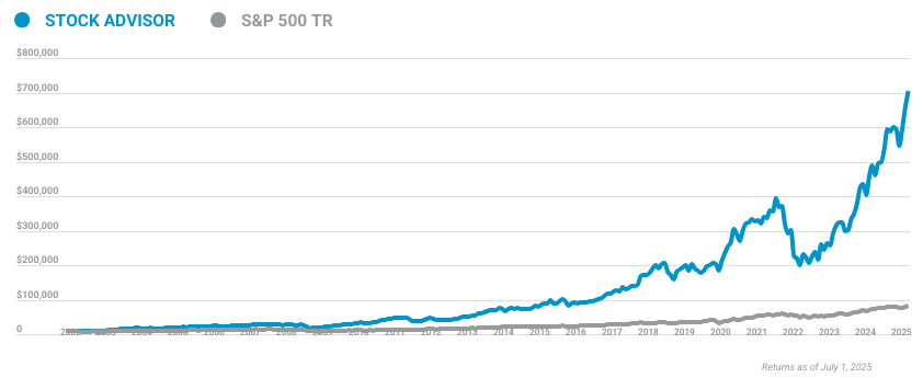
When investing geniuses David and Tom Gardner have a stock tip, it can pay to listen. After all, the newsletter they have run for over a decade, Motley Fool Stock Advisor, has tripled the market.*
David and Tom just revealed what they believe are the ten best stocks for investors to buy right now... and Atomera Inc wasn't one of them! That's right -- they think these 10 stocks are even better buys.
*Stock Advisor returns as of February 24, 2021
These forward-looking statements, whether in prepared remarks or during the Q&A session are subject to inherent risks and uncertainties. These risks and uncertainties are detailed in the risk factors section of our filings with the Securities and Exchange Commission specifically in the Company's annual report on Form 10-K filed with the SEC on February 19, 2021. Except as otherwise required by Federal Securities Laws, Atomera disclaims any obligation to update or make revisions to such forward-looking statements contained herein or elsewhere to reflect changes in expectations with regards to those events, conditions and circumstances. Also, please note that during this call we will be discussing non-GAAP financial measures as defined by SEC Regulation G.
Reconciliations of these non-GAAP financial measures to the most directly comparable GAAP measure are included in today's press release, which is posted on our website. Now, I would like to turn the call over to our president and CEO, Scott Bibaud. Go ahead, Scott.
Scott Bibaud -- President and Chief Executive Officer
Thanks, Mike, and welcome all of you to our Q1 update call. The last three months have been very interesting for our industry with the economic rebound driving semiconductor demand to the point where it's constraining industrial production across many different market segments. Fabs are once again running at or beyond their rate of capacity, which as you might expect, has had an effect on Atomera's efforts. For existing customers of wafers in process right now we are seeing no major changes but for those planning new experiments, we're hearing a potential delayed starts or extended processing times as production backlog takes first priority.
That being said, all of our existing customers continue moving forward on their development work with us. During discussions of incremental our new customer projects, we have started to hear rumblings of restrictions on R&D wafers because of tight capacity. At the same time, we are seeing increased requests to understand how MST can grow production volume through die size optimization. The current industry problems are a mixed blessing for us.
It's helping to spread the word on the economic benefits of MST while potential new customer work that validate our solutions is difficult to get started. We were pleased during this last quarter to be able to show our first customer entering into phase four. As a reminder, phase four is defined as the customer installing MST in their own facility. For a customer to enter into phase four, a number of factors have to be properly aligned.
First, the customer has to conclude that MST is worth the time and expense of dedicating a very expensive tool to its use. Second, they need to have at least one chamber available to work on MST that either means doing some modifications to run MST in a dedicated chamber on an existing machine or buying and installing a new one, so they can work with MST. Because tools dedicated to R&D are relatively rare in the industry, its generally much easier for customers to introduce MST on building out a new fab or adding to an older one. So, you can see that this phase four installation we achieved is no small feat.
Our licensees continue to move forward toward commercialization with MST and we have several other phase three customers who we hope will move in that direction soon. That being said Atomera works with very large companies in an industry that can move quite slowly even when excited about new technology. We've consistently said in the past that phase three is very unpredictable, which makes it difficult to provide guidance on when the next deal, be it a JDA or standard license will occur. Although, we continue to discuss JDAs with several customers, we are not in the late stages of negotiations on any at this time.
Beyond the JDA, all customer engagements continue moving forward. A focus on existing customers, ongoing travel restrictions and R&D wafer limitations will keep new customer growth from expanding significantly in the near term. However, we have been experiencing solid interest from both new and existing customers to learn how MST can be used in to expand their production volume and help solve both current and future capacity issues. It has been well reported in the news that many of the world's manufacturers have experienced production stoppages for the lack of the semiconductor chips necessary to build their products.
The automotive industry gets the most press, but same thing is actually happening in many areas of manufacturing. Semiconductor industry veterans that I've spoken with say this is the single worst shortage condition they've experienced in careers of over 30 years. It's worth the effort to dig a little deeper into the cause of this situation to understand the potential opportunity. Semiconductor companies are very focused on building out process technology for the next generation of semiconductor chips.
Indeed, this year we've heard about over $200 billion in investments to be made in semiconductor manufacturing, the vast majority focused on the bleeding edge. That will ensure that our mobile phones, PCs and servers continue to get full supply of the fastest and most powerful chips needed for those applications. But what is plaguing the industry today is a shortage of capacity and older process generations that make the necessary chips more mundane unless cutting edge applications like power management, sensors, microcontrollers and transceivers for automobiles, industrial products, communication gear and appliances. Typically, these products were designed in process nodes that went into production decades ago.
For certain designs using a lot of analog circuitry, it doesn't make sense to shrink to a smaller node. Yet, the fabs that produce these chips are maxed out and have a very hard time adding equipment to supplement their capacity. All the tricks available to get a few more wafers per hour out of these facilities were implemented years ago. Nevertheless, they keep trying to marginally increase output.
One way they could get significant relief would be to use MST. Let's look at a few different ways MST can be used solve industry problems. According to IC Insights, in 2020, more than 40% of monthly wafer capacity was to process nodes at 40 nanometers or above where more than half of that 180 nanometer or above, a manufacturing technology first introduced in the 1990s. Another 11% is in 20 to 40 nanometers, which the industry also categorized as legacy nodes.
These are the areas where the most help was needed, and MST is one of the only technologies with an ability to provide significant improvements in performance and die size for products in those process nodes. On this slide we show how at 180 nanometers MST SP is able to outperform an industry-standard designed by more than 30%. If we take those same mechanisms and direct them to die size reduction, MST is able to shrink a similar die by approximately 15 to 20%. Our ongoing development work continues to find ways to use MST to improve these numbers and thus, the expected savings.
Now, imagine an older fabs is very tightly restricted during the amount of wafers they can push through the building. The step function and costs to build a new facility is too large to consider but by encouraging their engineers to make new designs using MST, they will get 15 to 20% more chips out of the same number of wafers produced without it. Our economic analysis shows this will have the effect of increasing both revenue and profits for the fabs and their customers, while also providing a healthy royalty to Atomera. Remarkably MST should work even better at nodes smaller than the ones we talked about before.
Why? Well, as the industry goes to the smaller gate lengths, they typically use much higher levels of dopant. As you may remember, one of the key characteristics of MST is that it helps to control dopant diffusion, which is more important as doping levels increase. Because of this, we believe MST can help to make transistors narrower in the nodes just about FinFETs that is the 20 to 40 nanometer area I mentioned earlier. This could likewise increase the amount of die one can squeeze onto a wafer increasing capacity once again.
Recently, we completed an analysis of how MST could be used to improve performance of 28-nanometer products. Using parametric improvements, we found through silicon experiments, we modified an industry-standard 28-nanometer PDK and ran SPICE simulations for several different types of designs. The results were compelling. MST showed higher electron mobility and better gate oxide integrity, allowing higher overdrive, which resulted in more than a 30% performance improvement.
We then traded off the performance improvement for die size reduction using MST on a typical NAND2 gate like the one shown here, it resulted in a 22 to 25% area reduction. Analog scaling with MST provided a 21% reduction. So, overall, you can see how these results can really move the needle on capacity improvement. We have been in discussions with many potential customers about using MST to help solve their production problems.
Now, it is true that for this to happen, MST will have to be implemented and new chip designs will have to enter the pipeline. So, it's not a quick fix. But the capacity problems we are seeing today are only slated to get worse in years ahead as the size of the market continues to expand, driving demand for these older process chips in factories that have very limited expansion option. Although the opportunity in legacy nodes is quite exciting for Atomera, MST technology is also very well positioned to solve problems for customers at the leading edge.
As manufacturers attempt to make transistors with the smallest geometries, it's important that junctions are sharp and well-defined. As Robert Mears' blog post pointed out last week, MST does a much better job of that than other methods the industry is currently trying. We have previously been worried that MST, while very thin, may still be too big for these applications, so we tried making it much thinner and it still worked beautifully. Over the next few weeks, we will have more information about this development on our website and you can be sure that our customers are going to be hearing about it as well.
Efforts continue in the process of qualifying the new state-of-the-art Epi capability at our facility in Tempe, Arizona. As part of this process, we have successfully demonstrated MST growth on our advanced epitaxial reactors validating a tool that will be used for process development and customer support for both 200- and 300-millimeter wafers. With this new tool at our disposal, in addition to development, we will be able to conduct parallel testing and validation of MST with customers in phase four. This industry-standard approach has been proven to expedite learning and qualification by customers.
We continue to be excited about the opportunities the 300-millimeter tool will open to Atomera. Today, greater than 65% of semiconductor industry revenue is driven by 300-millimeter wafers, so having this capability will allow us to drive some very innovative business experiments to advance MST in the market. Our MST CAD software continues to be well-received by customers and partners. Just as important, it has opened up the ability for our engineers to experiment with different integration options without having to wait for silicon runs to validate them.
Here's three benefits we recently have realized with MST CAD. First, we've identified an improvement that we believe is significant for integrating MST with RF SOI by using a three-dimensional method of TCAD simulation. Second, MST CAD has helped us to advance our MST SP work much more quickly than we would have otherwise. Third, we are now also using it to evaluate different film types to optimize performance under different process conditions.
Overall, the development work we've done on MST CAD over the last several years is paying back giant dividends. As you can see our opportunities abound, it's critical that we not lose focus on the most important objective for Atomera though as we work to expand our efforts in multiple areas, and that is to get MST into production. It is for that reason that we spent time this year looking to supplement our team with an aggressive engineering manager with a reputation for execution who also had the background to understand and guide our efforts in these many areas. We are very pleased to have Sudarsan Srinivasan join Atomera.
His prior experiences at Applied Materials, Intel and Lam bring a wealth of experience that we believe will accelerate and focus our efforts. He has only been on the job for a few weeks but is already bringing some excellent insight that will help to drive better performance of Atomera in the future. Atomera continues to make strong progress on several fundamental applications we've been addressing for some time, but we also see more and more opportunity to tackle industry challenges with a film that brings a variety of benefits. With the strong technology base and a growing set of solutions we can provide, Atomera is currently very well positioned to navigate the road to a bright future.
Now, I will turn the call over to Frank to review our financials.
Frank Laurencio -- Chief Financial Officer
Thank you, Scott. At the close of the market today, we issued a press release announcing our first-quarter 2021 results. This slide shows our summary financials and I will now review them in more detail. Our GAAP net loss for the three months ended March 31, 2021 was $3.6 million, which is $0.16 per share.
In the first quarter of 2020, our GAAP net loss was also $3.6 million and on a per share basis, it was $0.22 per share. The flat net loss compared to Q1 2020 was due to higher revenue, which offset an increase in operating expenses. The lower loss per share reflects an increase in weighted average shares outstanding to $22.1 million in Q1 2021 from $16.8 million in Q1 2020. Revenue in Q1 2021 was $400,000 compared to $62,000 in the first quarter of 2020.
GAAP operating expense in Q1 2021 was $4 million compared to $3.7 million in Q1 2020, an increase of $276,000. Research and development expenses increased by $167,000 while general and administrative, and sales and marketing expenses increased by $68,000 and $41,000, respectively. Our press release and this slide contain a reconciliation between our GAAP and non-GAAP results. As has generally been the case for us, the biggest difference between GAAP and non-GAAP expenses is stock compensation, which is a non-cash item.
Our stock compensation expenses were $731,000 in Q1 2021 compared to $629,000 in Q1 2020. Non-GAAP adjusted EBITDA in Q1 2021 was a loss of $2.9 million, which is the same as in Q1 2020 as increased revenue offset our higher operating expense. Total non-GAAP operating expense was $3.3 million in Q1 2021 compared to $3 million in Q1 2020. Non-GAAP R&D expense was $2 million compared to $1.8 million in Q1 2020, an increase of $171,000.
This was primarily due to an increase $330,000 in payroll and related expense based on a new headcount in engineering, offset in part by lower outsourcing and travel costs. Non-GAAP G&A expense in Q1 2021 was $1 million compared to $927,000 in Q1 2020. Non-GAAP sales and marketing expenses were $213,000 in Q1 2021 compared to $192,000 in Q1 2020. Sequentially, our GAAP net loss was $3.6 million in the first quarter of 2021, which was $256,000 lower than our Q4 net loss of $3.9 million.
GAAP net loss per share was $0.16 in Q1 2021 compared to a loss of $0.19 per share in Q4 2020, reflecting lower net loss as well as a higher share count. Non-GAAP adjusted EBITDA in Q1 2021 was $2.9 million compared to $3 million in Q4 2020, reflecting our increased revenue offset in part by the increase in operating expense. Cash balance at March 31, 2021 was $36.7 million compared to $37.9 million at December 31. Net cash consumption of $1.2 million during Q1 reflects the use of $3.9 million in operating activities offset in part by $2.8 million in cash from financing activities consisting of $2.5 million of proceeds from the exercise of stock options and proceeds from the completion of our at-the-market or ATM equity program in January.
As in past years, our operating cash consumption is typically highest in the first quarter due to the timing of annual commitments, which are expense quarter. As of March 31, 2021, we had 23.1 million shares outstanding. Our JDA customer entered into phase four and obtained a manufacturing license enabling them to deposit MST using a tool in their fab. This license grant accompanied by delivery of our MST film recipe resulted in $400,000 of license revenue for Atomera.
The JDA includes other milestones that could result in additional revenue in the future. We do not have enough visibility to forecast the timing or likelihood of achieving those milestones. Consistent with past practice, we are only providing revenue guidance for this quarter, which we expect will be zero. Until we reach distribution license agreements that generate royalty, our quarterly revenues will remain choppy and our visibility will continue to be limited.
During periods of high capacity utilization, it can be even more challenging to schedule wafer runs that generate engineering service as well. And the timing of those transactions like the closing of new licenses or signing JDA is hard to predict. We continue to expect that our non-GAAP operating expenses for 2021 will be in the range of 14 to $14.5 million for the full year. With that, I will turn the call back over to Scott for a few summary remarks before we open the call up for questions.
Scott?
Scott Bibaud -- President and Chief Executive Officer
Thanks, Frank. I'm glad to share with you our latest opportunities and the progress we've made to-date. We are very excited about continuing to advance our JDA MST SP and RF SOI customers, and to begin work in the new areas highlighted on this call. We do see the current industry capacity challenges is creating an even stronger demand for MST technology and we hope to take advantage of it over the next few quarters.
As our new world-class Epi deposition tool comes online and MST CAD is adopted by more customers, we believe we'll be able to get customers through the integration process into markets more quickly than ever before. Inside Atomera, our teams are energized. We are working hard to realize the potential that MST brings, and I look forward to sharing the results of those efforts with you in the future. Mike, we will now take questions.
Mike Bishop
All right. Thanks, Scott. We will now enter the Q&A session. [Operator instructions] Our first question comes from Cody Acree of The Benchmark Company.
Cody, unmute and turn to the camera.
Cody Acree -- The Benchmark Company -- Analyst
Yeah. Thank you, Mike. I guess, Scott, if we could go back to your discussions about the engagements with your customers and the delays or maybe it sounds like almost tabling of some of your efforts. I guess, how direct have those customers been, have they given you any quantification? Has it been just kind of an engineer to engineer thing is or are you having communications at the C-level or division level that is giving you pause as far as just their ability to split attention?
Scott Bibaud -- President and Chief Executive Officer
Yeah, Cody. So, far there has been no pausing or tabling of our efforts with customers. What's happened is, if we have a customer that we are in phase three with and we're running wafers with them and the wafers are already in the fab, typically this -- those are -- they haven't really changed in priority and will get those wafers out and begin testing. But some customers who we were starting -- we were planning to do new wafer starts, let's say in a few months, they've told us they're not sure they'll be able to start on time and we'll see about that.
My guess is on most of those will probably start maybe with some delay and then move more slowly than we would have seen in the past. The bigger issue is for new engagements and new customers where they say, well, I think your technology is really interesting and we want to try it out in this area, but I can't get approval at the start of new R&D programs that will require wafers for some time into the future. So, summary is that for our existing customers, existing programs is not a huge program -- I mean, not a huge impact maybe some slight delays but for newer customers or even newer programs and existing customers it's a little bit harder right now.
Cody Acree -- The Benchmark Company -- Analyst
Sure. And Scott, you had shifted your attention from new customer acquisition to monetization of your customer program, so are you seeing a material -- you said you're talking about slight impacts of your existing customers or are you counting on those customers to increase engagements and that maybe solidify their interest? So that --
Scott Bibaud -- President and Chief Executive Officer
Yeah. The most important thing for us with existing customers is to get programs that we're working on now push to completion and get into production. Although it's great to start new programs with existing customers because generally you can get started faster, there's lower barriers, you don't have to go through all the formal contracts and so forth. But given a choice we'll try to push our existing programs to production as best as we can rather than starting new ones.
Cody Acree -- The Benchmark Company -- Analyst
Sure. You said you put more on your blog about your MST developments, you've not mentioned a thinner layer. Can you expand on that at all here?
Scott Bibaud -- President and Chief Executive Officer
Sure. So, our MST is quite thin. I think we say in our annual report that it's on the order of 100 angstroms or less. That's quite small.
10 nanometers or less but now the new -- the newest process nodes are talking about coming along at three nanometers or some fraction of that. So, even though MST is very, very thin we had a question about whether it would be -- some people had questions about whether it'd be applicable at those levels because that those levels they have a really dire need for the type of benefits that MST brings. And so, recently we started some development work on films that are very, very thin and we found they still have a lot of -- they have very good effectiveness and this is information that just really came out internally in the last week or week and a half, so we haven't had a chance to really publicize it and start to get out to the new customers about it. But Robert wrote his blog and we're working on white papers and other information and then going up to the leading customers to talk about that.
Cody Acree -- The Benchmark Company -- Analyst
And then lastly for me, just the process, the recipe that you mentioned in the press release that you were able to deliver, knowing that every customer is different what has been the -- I guess, what have you learned from the delivery of that recipe that you can port to other customers or is that not a tailored process that's not necessarily applicable across the board?
Scott Bibaud -- President and Chief Executive Officer
No. In this case we're delivering our -- really in many ways the company's crown jewels is our recipe for how you actually build the film in an epi tool. Even if you look at all of our patents and they talk about how the film is constructed, it's very, very hard to build. There's a lot of know-how involved in it, so that's what we deliver to the customer.
We've actually experimented in the past with delivering that to someone else to make sure we worked out the kinks and so this one went very smoothly so far. And I think we feel comfortable that we put together a process and a package to be able to deliver that to -- successfully to new customers in the future.
Cody Acree -- The Benchmark Company -- Analyst
Great Thank you, guys, very much.
Mike Bishop
All right. Thank you, Cody. Our next question comes from Richard Shannon of Craig-Hallum. Richard, if you want to unmute.
Go ahead and ask your question. Feel free to turn your camera as well.
Richard Shannon -- Craig-Hallum Capital Group LLC -- Analyst
Excellent. Thank you, Mike. And thanks, Scott and Frank, for taking my question. Unfortunately, I missed a lot of the call, so I didn't get a lot of your prepared details.
Based on Cody's question, I'm probably going to broach what he was talking about a little bit here. But it sounds like you're seeing some limits to the pace of progress given that most of the fabs out there are so full that there is not much room to run any test wafers here, is that a fair description of what you're seeing here in this current environment?
Scott Bibaud -- President and Chief Executive Officer
Yeah, I was telling Cody that we are still able to run test wafers that were in progress but getting new wafers especially for new projects started is becoming more challenging. And I would say on my last update call, which was in early February, we were not seeing that. It's just been something that -- and we are watching for it because even at the beginning of the year the answer is heating up, but this is something we've just in the last couple of months.
Richard Shannon -- Craig-Hallum Capital Group LLC -- Analyst
OK. Are you able to run wafers on projects that have already been started and your customers are very interested like your phase four customer, as an example? Is there any limits to doing that or can you push those through on the original time frames that you're expecting?
Scott Bibaud -- President and Chief Executive Officer
So far, we haven't heard about any delays on any of those programs.
Richard Shannon -- Craig-Hallum Capital Group LLC -- Analyst
OK. Are you worried about that, is that giving you some pause, or you feel pretty confident your customers are going to show your wafers to run on schedule?
Scott Bibaud -- President and Chief Executive Officer
Yeah, I mean, we've lived through this before. I think there were some delays but to the extent that we were able to make people excited about it is they continue pushing it forward with some delays. I think the fact is, we're not super focused on bringing on new customers right now and if we did then that would be a bigger issue because starting a new R&D program that requires wafers is challenging. But I think the bigger -- the more interesting thing is that a lot of the engineering management of our customers has now turned their attention to trying to figure out how to expand their capacity through innovative means help solve some of these capacity issues not right now -- I mean, not only right now, but also in the future.
As you know, there have been a number of forecasts for the semiconductor industry that we're going to grow from about a 450 to $500 billion market today to about a $750 billion market in 2027. And that type of growth is going to come with demand for the same type of chips that are having capacity problems today. So, if the capacity problems don't get solved in the next six to nine months they still are going to have to be solved over the next few years and MST brings a lot of really strong tools to be able to do that for customers. So, I hope that during this capacity crunch it drives demand to us to start working with customers to understand how MST can be useful to them then designing experiments that will run when the capacity becomes available again.
Richard Shannon -- Craig-Hallum Capital Group LLC -- Analyst
OK. Scott, anything that Atomera can do to make progress particularly at the customers who were far all along the pipe. I know that you've talked I think for this a couple of quarters about focusing more on those and less so on adding new customers at the early phases here, is anything else you can do or encourage your customers, anything you can do to kind of keep that pace going, especially for leading for the farthest along edge of customer base?
Scott Bibaud -- President and Chief Executive Officer
Yeah. One of the things that has been very helpful to us along those lines is our MST CAD. A lot of the phases that we talk about when we talk about working with customers are designed around physically processing wafers and moving wafers through toward production. But you can do a lot of that with MST CAD just through simulation and that's not something that we had available to us a few years ago.
So, now even during a period when a customer says, well, we can't -- it's going to be a delay in running these wafers that's going to give us a few more months to just be running simulations that can find better and better solutions. So, when we do get the wafers, we'll have a higher probability of having success. So, yeah, that's definitely one way that we can continue working with customers even through capacity issues.
Richard Shannon -- Craig-Hallum Capital Group LLC -- Analyst
OK. Sorry, one last quick question from me is with your phase four customer that is, as of today, is on announced in terms of name. Is there any thoughts on when this customer might be announced in terms of Phase or what Phase to enter getting to production or anything like that? Trying to get a sense of when we might figure out who they are.
Scott Bibaud -- President and Chief Executive Officer
This customer is extremely sensitive about confidentiality and I'm not sure when they would actually start to loosen some of that up considering the amount of focus that they've had on that. At some point when we do go to production, I think it will become intuitively obvious, but for now, I don't think they're going to want to say their name in the near term. And one of the things I should -- we never talk about specific customers and where they are in the development phase, all of them are sensitive to that type of thing. One thing I want to make clear about this JDA customer is, I've seen a lot of questions coming in about how fast they'll move in from phase four and into phase five but for a JDA customer like this, the work that we're doing is really a mixture of kind of phase three and phase four.
They've installed in their fab, that's great. It means they can deposit MST in half an hour as opposed to a month if they have to send it to us for us to process but they still are going to be going into the phase three process of trying MST on a number of different applications and proving it out before they decide to make it available to the business units. So, they might be able to try it a little bit more and then take it into production. So, I know you didn't really exactly asked for that level of detail, which I'm just seeing there's a little confusion out there.
I want to try to clear it up.
Mike Bishop
All right, Scott, why don't we go ahead and move to the Q&A that's been typed into the chat here. And the first question comes from William Morrison and he is asking if MST CAD is gaining traction with the customers, and is it accelerating the conversation then moving customers along the pipeline?
Scott Bibaud -- President and Chief Executive Officer
Yeah. As a matter of fact, I'll tell you one of the interesting things that's happening is -- it used to be we would go to customers and we'd have our first conversations, we get into kind of deep discussions about physics and how MST works and how it can be integrated in their product. And then, we would start working on a plan to put it on the wafer, so they can test them and see how well it works in their fab. Today when we go to customers and we have those same type of discussion they instead of talking about building wafers right away we start talking about doing some MST CAD simulation.
So, it's much lower barrier for customers to try out our technology and hopefully, we'll get them to make -- when they do they make their wafer runs some higher probability of having success right from the start. So, we've had really good luck with that. I think on almost every discussion we have with new customers or with our existing customers now, we're leading off talking what MST CAD and that's been very helpful for load time.
Mike Bishop
All right. And then, we've had a number of questions on the Epi tool. Is it qualified, where is it, is it going to be used by your JDA partner and the timeline on that? So a number of investors have asked that question, so why don't we address those?
Scott Bibaud -- President and Chief Executive Officer
OK. So, our Epi tool is located at the Arizona State MacroTechnology Works center in Tempe, Arizona. It's a world-class semiconductor facility used to be owned by Motorola, who I believe transferred it to Arizona state years ago. Beautiful state-of-the-art facility.
Now, why in Tempe, which is just outside of Phoenix? Phoenix is a little bit of a epitaxial center of excellence in the world. That's where there are a lot of engineering -- a lot of engineering town out there that does that. It's also a site of a number of fabs. And when you run Epi you need to have the infrastructure that you need for a semiconductor fab including very large hydrogen tanks and other chemical suppliers that are nearby.
Our tool is set up. We are actually processing wafers in there and we're qualifying our film. All that being said, we haven't signed off a 100% on the full facility requirements yet. I know it's been a long time, it seems like we're always right around the corner.
I just -- it's hard to understand -- yes, we have this -- there is the wafer processing capability and then there's a whole bunch of surrounding equipment that has to do with metrology and cleaning tools and air handling and a whole bunch of other things that have to all be qualified before we take possession -- official possession of the tool. And I feel like we're very, very close on that but isn't quite fulfilled yet. I guess the upside of that is that we haven't started hitting on our lease yet. The downside is that we don't feel comfortable delivering wafers to customers until we've taken -- until it's met all of those criteria.
When we do have that met and I -- again, I do hope it's soon we will have the ability to run customer wafers there or even make -- well, we'll definitely be running our own internal R&D wafers there, and we will have the ability to build wafers ahead of time and seed them into the market and other things to try new business approaches.
Mike Bishop
All right. And the last category of question deals with the chip shortage and if it got the -- it seems you have gotten the attention of the federal government and so the question is, do you see any federal government agencies that you're working with to help you advance your goal or is that not on the radar at this point?
Scott Bibaud -- President and Chief Executive Officer
Yes, we don't -- we haven't really approached government agencies regarding that. We are -- there's other reasons why we might be talking to government agencies about our technology for our use in various applications, but for -- to help solve the current capacity expansion that hasn't been something that we have done up to now.
Mike Bishop
OK. So, at this point, I think that concludes the Q&A session. I'll turn it back to you Scott for closing remarks.
Scott Bibaud -- President and Chief Executive Officer
All right. Well, thank you, Mike, and thank you all for the good questions. And also thank you for attending today's presentation. We are very pleased to be able to share with you the results of our last three months and provide a sense of the excitement we feel inside Atomera.
Please continue to look for our news articles and blog posts to keep you updated on our progress. You can sign up with them along with investor alerts on our website atomera.com. Should you have additional questions please contact Mike Bishop, we'll be happy to follow up. We look forward to seeing some of you during our scheduled marketing activities, including the Stifel Cross Sector Insight Needham Technology and Media and Oppenheimer Emerging Growth conferences.
Thanks again for your support, and we look forward to our next update call.
Mike Bishop
All right. And that concludes today's call. You may all disconnect.
Duration: 44 minutes
Call participants:
Mike Bishop
Scott Bibaud -- President and Chief Executive Officer
Frank Laurencio -- Chief Financial Officer
Cody Acree -- The Benchmark Company -- Analyst
Richard Shannon -- Craig-Hallum Capital Group LLC -- Analyst