Image source: The Motley Fool.
Atomera Inc (ATOM -0.87%)
Q2 2022 Earnings Call
Aug 02, 2022, 5:00 p.m. ET
Contents:
- Prepared Remarks
- Questions and Answers
- Call Participants
Prepared Remarks:
Mike Bishop
Hello, everyone, and welcome to Atomera's second quarter fiscal year 2022 update call. I'd like to remind everyone that this call and webinar are being recorded, and a replay will be available on Atomera's IR website for one year. I'm Mike Bishop with the company's investor relations. As in prior quarters, we are using Zoom, and we will follow a similar format with participants in a listen-only mode.
We will open with prepared remarks from Scott Bibaud, Atomera's president and CEO; and Frank Laurencio, Atomera's CFO. Then we will open the call for questions. If you are joined by telephone, you may follow a slide presentation to accompany our remarks on the Events & Presentations section of our Investor Relations page on our website. Before we begin, I would like to remind everyone that during today's call we will make forward-looking statements.
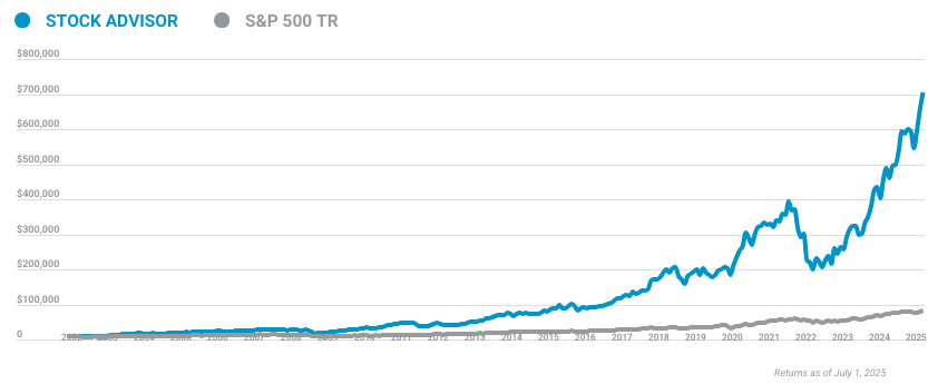
10 stocks we like better than Atomera Inc
When our award-winning analyst team has a stock tip, it can pay to listen. After all, the newsletter they have run for over a decade, Motley Fool Stock Advisor, has tripled the market.*
They just revealed what they believe are the ten best stocks for investors to buy right now... and Atomera Inc wasn't one of them! That's right -- they think these 10 stocks are even better buys.
*Stock Advisor returns as of July 27, 2022
These forward-looking statements, whether in prepared remarks or during the Q&A session, are subject to inherent risks and uncertainties. These risks and uncertainties are detailed in the Risk Factors section of our filings with the Securities and Exchange Commission, specifically in the company's annual report on Form 10-K filed with the SEC on February 15, 2022, and in our prospectus supplement filed with the SEC on May 31, 2022. Except as otherwise required by federal securities laws, Atomera disclaims any obligation to update or make revisions to such forward-looking statements contained herein or elsewhere to reflect changes in expectations with regards to those events, conditions, and circumstances. Also, please note that during this call, we will be discussing non-GAAP financial measures as defined by SEC Regulation G.
Reconciliations of these non-GAAP financial measures to the most directly comparable GAAP measures are included in today's press release, which is posted on our website. Now I would like to turn the call over to our President and CEO, Scott Bibaud. Go ahead, Scott.
Scott Bibaud -- President and Chief Executive Officer
Good afternoon, and welcome to Atomera's second quarter 2022 update call. Once again, we've had a very productive quarter with the progress I look forward to sharing. Then after discussing how the newly passed CHIPS Act affects us, I'll turn the call over to Frank to review our financials and outlook. In the first quarter, we saw our existing customers reinvigorated by the ability to start new wafer runs as fab capacity started to open up.
The second quarter was where new customer interest in projects with existing customers have really started to grow again. Atomera received a lot of inbound interest from customers of the industry's most important power and RF-focused trade shows as well as the large VLSI and Semicon West Conferences held over the last three months. These were great forms for Atomera to have the in-depth technical conversations necessary to deepen existing relationships and gain a foothold with new customers. We are starting to see the fruits of those efforts with our new addition to our customer pipeline.
We expect that trend to continue as the number of targeted applications increases and R&D wafer runs become more accessible as fab capability continues to loosen up. The bigger news is that progress with our customers in phase 3 is going particularly well. We have a number of important wafer underway with licensees, JDA partners, and other customers, which hopefully will yield results encouraging them to move on to more licensing phases and ultimately into production. Although none of those lots are finished, we have been able to look at some data prior to lot completion and have been very encouraged by the promising interim test results.
As you know, we use MSTcad with customers to predict what kind of improvements they will see. Early indications are that the TCAD simulations which showed enough potential to initiate customer wafer starts are closely predicting the measured silicon improvements, and in many cases, the actual results are exceeding both our expectations and those of our customers. Results may vary when the final test data becomes available, so we must be patient, but those early results have folks very excited. Programs with all our licensees and JDA partners continues to make good progress with the exception of AKM, which is still recovering from a fab fire.
As you can see from this chart, we now have 26 engagements with one new addition to the first phase. One customer has been in phase 2 longer than normal, which reflects an extended experiment they are conducting in that phase, different than those done by most customers. We believe that results from this effort will lead to a deeper engagement into licensing and production opportunities. There are two important factors determining how fast Atomera make progress with new and existing customers.
Our ability to meet face-to-face to gain trust and credibility, and then our customers keep capacity to start R&D wafers in their fabs. For the last two years, we've been held back on both fronts. Today, we can travel freely in the U.S. and with only a few restrictions in Europe.
So, far, travel in Asia has been slower to recover, but our first trips over there have gotten underway this quarter. Industry capacity constraints are starting to soften, which is a positive for Atomera, but this trend is not uniform. While memory manufacturers and mature nodes that IDMs and foundries are starting to loosen up, manufacturers of the most advanced nodes are still highly impacted. So, R&D starts in that area are still hard to come by.
Our goal is to take advantage of lower travel restrictions to get MST wafers started in as many customer fabs as possible and to build on the momentum we experienced in the first half of this year. We are seeing clear signs of interest in our technology across certain segments of the industry, displaying the domino effect I've spoken about in the past. Engineers are more comfortable using a novel technology if it's being used by others, and we believe this is being initiated because of industry chatter, even before anyone has gotten into production. In particular, our work on RF-SOI, a technology which is critically important to the 5G cellular market, is something which has interest across the sector because of its ability to solve a difficult industry problem.
5G cellular devices can have up to 10 times the content of RF components as older 4G devices. At the same time, we have consistent feedback from customers that continued improvement in key RF devices such as switches and LNAs are increasingly hard to come by with internal process tweaks. Accordingly, the payoff to customers who can implement industry-leading RF device performance should be very significant. So, the interest from our customers in using MST to deliver such improvements is very exciting.
Work with multiple customers is also underway with MST-SP for power devices at five volts and above. This is an area that will exhibit continuous growth over the next decade due to the emphasis on battery operation in electric cars, and we believe Atomera will benefit from this trend. Now, I'd like to take a few minutes to explain a quite important new discovery we've made on MST for advanced nodes. Atomera's technology is remarkable in the number of different benefits it can bring to semiconductor devices, and it does so through several mechanisms, including, importantly, enhanced electron mobility.
While the electron mobility improvements have been confirmed for many years, the underlying physics behind how MST delivers those enhancements have not been fully understood. In silicon devices, electron mobility can be impeded through three different types of electron scattering; coulombic, phonon, and surface roughness scattering. Until recently, our assumption was that at very advanced nodes, MST primarily improved bone on scattering, leading to about a 5% overall improvement in electron mobility, which is good but may not drive stand-alone adoption. Recently, we completed some characterization of MST devices at temperatures near absolute zero, which gives us a unique ability to separate out MST's impact on each scattering component.
To our surprise and delight, it showed that MST enhanced electron mobility related to surface roughness scattering by over 50%, which is a massive improvement and something particularly important in the advanced nodes. OK. This is just one factor in a complicated transistor design. But the net result is that this new ability for MST to smooth the surface can bring greater than a 15% electron mobility improvement to the most advanced semiconductor processes.
As the process node gets smaller, the MST benefit is large, which means that MST for only a modest incremental cost could deliver a full node of performance improvement. Now that is something that would be very compelling to designers working on the latest two or three nanometer gate-all-around transistors. Because this result is so new, a full peer-reviewed journal article will not be available for some time, but today we did post a white paper describing the phenomenon in much more detail on our website, and this will be used to start discussions with our advanced node partners. Although a bit technical for most investors, it does provide an excellent background on our technology and explains the significant potential benefit for customers on advanced nodes.
When a breakthrough in MST like this one is achieved, our team then goes to work documenting how it can be used in different applications. This is a valuable IP that forms the underpinning of Atomera's business model, and I'm pleased to report that as of the end of Q2, we have reached 318 patents granted and pending with particularly strong growth in our foreign patent portfolio. As the industry has come to understand the benefits of MST and how they might use it in their own future designs, it is becoming increasingly common for them to refer to our technology in their own patents. This is a positive development for Atomera as it not only validates MST's innovative value to the industry, but it also opens another path of dialogue for us and the customer.
Last week, Congress passed the CHIPS and Science Act, a $280 billion package that includes $50 billion in funding to develop and enhance domestic semiconductor manufacturing capability. Among the many reasons for passing this legislation is to make U.S. companies better at implementing the most advanced technology nodes we've just been talking about. But $2 billion of the Act was specifically allocated to improving legacy chip production, which is one of the key areas where MST provides a rare and much-needed boost to the industry.
Atomera will be working with CHIPS Act administrators and our U.S. legacy fab partners to educate them on how our technology can improve existing fab capacity, throughput, and performance while improving their profitability. MST can enable those legacy fabs to meet the goals of this new legislation now, not sometime in the future, and we believe CHIPS Act funding can help subsidize the cost of MST implementation at our fab partners. The CHIPS Act also initiates or strengthens several R&D initiatives important to Atomera, including the National Semiconductor Technology Center and our academic partners efforts.
Government advocacy for improving the U.S. semiconductor manufacturing prowess is another tailwind in conjunction with strong industry capex growth plans that will be a positive for Atomera as they both provide important catalysts for adoption of our technology. The CHIPS Act is capped off three months of intensive customer and R&D progress. The many wafer runs we have underway are progressing well and preliminary results look very promising.
Our team is on the road and new customer activity is starting to pick up. Inside the company, we are meeting milestones, generating new and innovative IP, and strengthening our team. I think we've accomplished a lot this year, but I also believe that the second half of 2022 will outshine the first because of the momentum we are carrying today and the customer opportunities in front of us. Next, let's have Frank review our financials.
Frank Laurencio -- Chief Financial Officer
Thank you, Scott. At the close of the market today, we issued a press release announcing our results for the second quarter of 2022. And this slide shows our summary financials. Our GAAP net loss for the three months ended June 30, 2022, was $4.5 million or $0.20 per share, compared to a net loss of $3.7 million or $0.17 per share in the second quarter of 2021.
In Q1 of this year, our GAAP net loss was $4.1 million or $0.18 per share. The sequentially higher net loss in Q2 2022 over Q1 was mainly due to the fact that we recognized revenue in Q1 of $375,000, but we did not recognize any revenue in Q2. At the same time, our operating expenses increased only slightly over Q1. GAAP operating expenses in Q2 were $4.4 million, compared to $3.7 million in Q2 of 2021 and $4.3 million in Q1 of this year.
Non-GAAP net loss for the second quarter of 2022 was $3.5 million, compared to losses of $3.3 million in Q1 and $2.9 million in Q2 of 2021. Non-GAAP operating expenses last quarter were $3.6 million, which was unchanged sequentially over Q1 and compares to $2.9 million of non-GAAP operating expense in Q2 of 2021. The increase in non-GAAP operating expenses in Q2 this year versus the same period last year was $697,000. This increase primarily reflects a $336,000 increase in R&D expense due to our 300-millimeter tool lease, which commenced in August of 2021, as well as increases of $170,000 in sales and marketing and $190,000 in G&A expenses.
Our cash balance at June 30, 2022, was $21.8 million, compared to $24.5 million at the end of Q1. We commenced our aftermarket or ATM equity program on May 31, 2022. And during the second quarter, we sold 31,652 shares at an average price per share of approximately $11.24, resulting in net proceeds of approximately $345,000 after sales commission. I'd like to point out that on our cash flow statement, Q2 ATM proceeds are listed as $185,000 in cash from financing activities because all expenses related to the initial setup of the ATM are netted against the proceeds in that period as required by GAAP accounting rules.
Similar levels of ATM-related expenses will not recur in future periods. As of June 30, 2022, we had 23.5 million shares outstanding. As Scott mentioned in his remarks, we've made good progress with our JDA customers and other engagements. At this time, we're not yet in a position to predict when we may reach revenue-generating milestones under our second JDA, which we announced last quarter.
We're very happy that preliminary results are promising, and we have increased -- and they've increased our confidence that this JDA will result in us reaching paid licensing phases and recognizing revenue. Since we cannot yet predict this timing, our guide for Q3 revenue is zero. And consistent with our past practice, we're not providing revenue guidance beyond the current quarter. On the last update on call in May, I guided the full-year non-GAAP operating expenses for 2022 would be in the range of $15.25 million to $15.75 million.
I'm happy to announce that we've added two new engineering head count in July, and we're catching up on our plans to grow our team. But as a result of these hiring delays, our expenses are trending lower than we originally planned, and are reducing the full-year guidance for non-GAAP operating expenses to a range between 14.75 and $15.25 million. With that, I'll turn the call back over to Scott for a few summary remarks before we open the call up for questions. Scott?
Scott Bibaud -- President and Chief Executive Officer
Thanks, Frank. The past three months have been very positive for Atomera with solid progress on the customer front and breakthroughs coming in R&D. Our team is growing, and the pace of innovation is exceptional. With in-person customer visits back underway, we expect to improve on the results we have delivered in the first half of the year, and our team is hard at work making that happen.
The macro trends in the industry, including strong capex in combination with the new CHIPS and Science Act, continue to provide a very favorable environment for MST adoption. We definitely believe we'll be reporting more good news soon, and I look forward to sharing it with you in the future. Mike, we can take questions now.
Mike Bishop
All right. Thank you, Scott. [Operator instructions] And right now, our first question comes from Richard Shannon of Craig-Hallum. Richard, if you would kindly unmute and turn on your camera, you may begin.
Richard Shannon -- Craig-Hallum Capital Group -- Analyst
Great. Thanks, Mike. Can you hear and see me?
Mike Bishop
Yes, we can.
Richard Shannon -- Craig-Hallum Capital Group -- Analyst
Excellent. Thanks, Scott and Frank, for having me on here. A lot of interesting commentary from the call, then no particular order here. One thing I did want to get was an update on the JDA contracts and Frank gave us a brief comment about.
I'm not sure when the second JDA will necessarily get to revenues here, but maybe you can talk about the progress here. I guess my two specific questions here are, with the first JDA, I think you're just working with a single business unit after having transitioned out of work with the central engineering organization, wondering if any progress there or multiple business units. And then, I guess, with the second JDA here, it sounds like you've made some progress overall here. Maybe you can just kind of add a little bit more color as to what progress you have made with the second one.
Scott Bibaud -- President and Chief Executive Officer
Yes. So, let me -- I'll start with the second one. So, I think we mentioned when we talked about -- originally talked about the JDA that we would be working with a kind of a lead business unit that was going to be pushing to move very quickly, and we have been pleased at the pace that things have been going. The industry is still somewhat impacted.
So, if we had a really -- we had more capacity available, I think we would have expected to move even faster, but good progress so far. But as I said in my commentary, we haven't gotten the final results. So, we don't really have a good insight into what will happen next. We've got most of the legal work done with -- yes, we've got most of the legal work done before we signed that JDA.
And so, we believe that we will move pretty quickly once we go from here. On the first JDA, we probably -- I can't give a lot of details about where we are with specific business units until they reach a milestone that we can announce something with them. I can tell you that we continue to work with that first JDA customer pretty intensively. And we're hopeful that we'll be able to get to a point where you can make some announcements of it later this year, but I can't really give much more insight than that.
Richard Shannon -- Craig-Hallum Capital Group -- Analyst
OK, fair enough. Scott, thanks for that. In the earlier part of your prepared remarks, Scott, you talked about some data from recent wafer runs that haven't been quite completed here. I guess one specific lead-in question to that topic here is I don't think you mentioned characterizing the technology or know that you are working on and whether this was on Atomera or customer infrastructure.
Scott Bibaud -- President and Chief Executive Officer
Yes, I didn't talk about that. But generally speaking, I'd say it's almost always on customer infrastructure. We can do kind of phase 2 type of setup and material characterization work with our customer on our equipment. But if we're doing phase 3, it really has to be on their equipment and their fab.
And so, that's really where it's been underway.
Richard Shannon -- Craig-Hallum Capital Group -- Analyst
OK. And how long before you get the full data? And can you kind of fully characterize what that really means here?
Scott Bibaud -- President and Chief Executive Officer
Yes. I don't want to talk about specific schedules. I'd say we're getting close. I expect to learn a lot more this quarter.
It might go out into Q4. And by the way, we're not just talking about one wafer run, we have a number of different wafer runs with different customers. And so, I expect that we'll be getting some data out this quarter and some of it will be coming later on. And hopefully, that will turn into more wafer runs from there.
Richard Shannon -- Craig-Hallum Capital Group -- Analyst
OK. Fair enough. In terms of the discussion that you had on the advanced nodes in the white paper that came out, I brought it up, but I probably read about two sentences before the call started here. This sounds like it's fairly early stage in terms of engagement here.
Is that a fair characterization of what's going on or is it more advanced than what I guess my interpretation?
Scott Bibaud -- President and Chief Executive Officer
I would say that the testing work, the R&D work is pretty advanced. We've gotten a lot of data, and I think we have enough to make this type of insertions, which we're not making -- we don't just make them flippantly based on a lot of simulations and so forth. But we don't have any ability to actually run wafers in the most advanced nodes to run experiments. We have to work with customers for that.
So, yes, I would say it's quite early in our engagements with customers on this. Now we have been talking to customers in the advanced notes about our technology. This can be used in many ways. But this is a new phenomenon that we didn't know about before that we think will be very interesting to people.
Richard Shannon -- Craig-Hallum Capital Group -- Analyst
OK. All right. That's helpful. In the past few quarters, and I know for just reviewing the transcript from last quarter, you talked about this basically in terms of RF-SOI.
And I think the comments you made on today's call was that if I caught this incorrectly, please correct me, but it sounds like you're having nearly full engagement across the industry for RF-SOI. Is that fair? And then also, do you still see that as a good candidate for the technology that takes you first across the finish line to volume production?
Scott Bibaud -- President and Chief Executive Officer
Yes. I don't know if I would say across the entire industry, but across a lot of the industry, absolutely. The word is out on our technology for RF-SOI and we're solving a problem that people have been struggling with for years, and everybody is trying to figure out. That is a very, very fast-growing market, a lot of innovation happening, and everybody is trying to figure out how to get the next leg up.
So, what we're talking about is a real potential game-winner there. Your second question about whether it would be the first to production, I've always said that we have been working on our power technology longer than RF technology. And so, some of our customers that are doing power work are longer in the tooth, but we'll see -- so I don't want to make a prediction, but I'd say we're probably one of those two that might be early to production.
Richard Shannon -- Craig-Hallum Capital Group -- Analyst
OK. That's fair. Perhaps it's my last question here, I'll think through this as I'm hearing your answer here. But one of your more interesting comments was that you think a lot of the interest coming into Atomera here recently is coming from industry chatter.
I assume it was more kind of anecdotal, but maybe you can just share why you said that, what you're hearing, and kind of the benefits that you're receiving from that.
Scott Bibaud -- President and Chief Executive Officer
Yes. Well, it's inevitable that we've been working in the industry for a while. If you're working at one customer and you're bringing them a big potential solution for a problem, there's going to be a number of engineers in that company that know about it. They might change companies, they might have friends, they might go to trade shows, they might actually see our presentation to start just chatting among them in a specialty that certain engineers will have chat rooms and things set up around.
And so, we are seeing that people from companies that are kind of reaching out to us unexpectedly because they heard from some other sources. And then -- and hopefully, that will lead us to some new engagements and some good opportunities. That's the type of thing that we expected to really happen once we got into volume production because customers are really risk averse, but we're starting to see it happen just based on chatter.
Richard Shannon -- Craig-Hallum Capital Group -- Analyst
OK. Interesting comments. I think that might be it for me. I'll jump out of the line, maybe I'll reenter here, but congratulations guys on what sounds like some great progress, and keep up the good work.
That's all for me.
Mike Bishop
All right. Thanks, Richard. And Cody Acree from Benchmark has his hand raised. Cody, feel free to go ahead.
Cody Acree -- The Benchmark Company -- Analyst
Yes. Thanks, Scott. So, I guess maybe if we can start with Scott, just on the capacity comments that you made for your 200- to 300-millimeter infrastructure? How is that running? I guess, you talked about utilization being a key driver to engagement. So, are you still running available capacity? Or are you at limitations now?
Scott Bibaud -- President and Chief Executive Officer
Yes. I mean, I would say, in general, I'm speaking more about our customers' capacity than our capacity to the extent that they want to run wafers with us, we find a way to make that happen with our infrastructure of it, with tools that we have in our two different Epifacilities. But as I was saying on the call, if our customers' fab is completely full, it's very hard for them to run any R&D wafers, we're starting to see that loosen, but more so in the older nodes and the legacy nodes and also in the memory area. Obviously, it's a well-documented kind of slowdown in memory area.
But for the most advanced nodes, they're still really, really old and it's hard to make as fast to progress as we would like with them.
Cody Acree -- The Benchmark Company -- Analyst
And you mentioned that you could only really run wafer characterization through phase 2.
Scott Bibaud -- President and Chief Executive Officer
So, phase 2 -- actually a good question because I mentioned a customer that is in phase 2 and has been there for a while. So, typically, our definition of phase 2, a customer sends us their wafers, we deposit MST on there. And then both we and the customer look at how MST physically integrates onto their wafer. And in most cases, this is a step that only takes a month, maybe a month and a half.
You deposit some and make a few tweaks and then it works fine, and you move forward with moving into phase 3 and running wafers. But some customers want to do much more complicated structures or patterns on their wafers, and they want to see how the MST deposits there. And in some cases, we need to do work with them to get it to turn out to work exactly the way that they would like it to. So, typically characterization of the MST itself is done in phase 2.
And from there we know that we're going to have a good deposition on our phase 3 rounds.
Cody Acree -- The Benchmark Company -- Analyst
Your comments on MSTcad, how important is this progress that you called it out in the press release, and that are you seeing more recent improvements in the characterization of your results? Or is this something that's been consistent, and you just called it out here on the specific program?
Scott Bibaud -- President and Chief Executive Officer
Yes. It's a type of thing that we did a -- we announced our first major release of MSTcad, I think a year and a half ago, but it's been continuously improved and improved. And some people in the industry can be skeptical of the results that you get on TCAD. It's such a complicated process that typically process engineers that work in the factories.
They say, let me just run wafers and look at the results because TCAD can be all over the place. It might tell me I'm going to get a big improvement and then when I run the wafers, I get a reduction instead. But what we have been seeing is that our TCAD that we've been working on so hard is actually validating the improvement that we're showing before him. And that's always what you need to build credibility in your simulation tools.
And so, yes, so that's been really, really gratifying to see because we can do a quick simulation with a customer before they run any wafers and show them what kind of benefits they can get. And then if we can say, OK, this works the last 10 times we tried it. And so, this is very accurate depiction, that's very helpful.
Cody Acree -- The Benchmark Company -- Analyst
Are you getting them to, I guess, accept your results as validation, or are they still at a stage where they're going to need their own internal wafers to check your results?
Scott Bibaud -- President and Chief Executive Officer
I think it's going to always be like a precursor to real wafers being run. But when you run wafers, you typically have -- you try a lot of experiments. So, if you don't believe the simulation, you could try 1,000 experiments and still miss what you're trying to do because you need to do 2,000, right? But if you use TCAD, it can help to narrow that down, so you need a lot fewer experiments to actually see the results that you're going after. And of course, to believe that and narrow down your set of experiments, you need to have faith in the TCAD results themselves.
Frank Laurencio -- Chief Financial Officer
Yes. I mean, if I could jump in on that because I sort of observed the dynamic that we've seen recently and that we talked about in the release and on the call about TCAD. You may have a situation where a customer is feeling marginal about the cost-benefit of doing another set of wafers, particularly recent times when capacity is tight and it's difficult to justify R&D runs. And as they see that the TCAD predictions are actually being validated in the experiments they do run, then it helps to build more trust in our models.
And if there's someone who is -- needs to be convinced or they want sort of further evidence to continue to run experiments in a particular direction, I think it's helped us to gain a lot more credibility with customers around trying other experiments with MST than they would have previously. So, I think seeing -- they'll always want to see it validated in silicon, but that dynamic helps to help our engagement with customers a lot. We've seen that playing out in real life.
Cody Acree -- The Benchmark Company -- Analyst
Thanks, Frank. And then lastly for you, I guess just with the CHIPS Act with there being a sizable portion toward R&D and legacy development, do you -- you mentioned on the remarks about endorsement or funding to your customers to reimburse for -- to cover their implementation costs. But is there any opportunity in the CHIPS Act that you understand that would be a direct beneficiary to you?
Frank Laurencio -- Chief Financial Officer
I think that it can. The allocation of a certain amount specifically called out for what they call sort of mature technology nodes in the CHIPS Act can be interesting. And these tend to be ones where if you can find an application that addresses an industry that's great kind of concern to the domestic economy like automotive products, which many of them are legacy technologies, I think that we could do that. We're still relatively small.
So, we're not of a scale where we engage in directly lobbying politicians. So, from my standpoint, the work for us begins more now in talking to folks about where, as I understand the process, you get into not just the approval of the funds, but now the appropriations bills to allocate that into specific programs. And so, I think that that's where we could be a direct beneficiary. So, I think that we're going to be only ramping up our efforts there even more.
Mike Bishop
Thanks, Cody. And I don't see any raised hands at this point in time, but we do have a number of questions that came in on the Q&A chat. And the first one is just basically a review of what the phases mean. And so, maybe, Scott, if you could review what the phases are for -- that we display in our charts.
Scott Bibaud -- President and Chief Executive Officer
Absolutely. Yes. I do have -- we do have formal definitions, but let me just talk them through. Planning.
So, planning is not like a big opening on a customer funnel that you would think of in a traditional sales funnel. Planning is once we have worked with a customer long enough that they have, number one, they've signed an NDA with us, meaning that they're going to start telling us about their manufacturing process. And believe it or not, these customers are very hard to get an NDA done with because they're very protective of that technology. Number two, they have to be actively planning on doing a wafer run with us.
So, they're in engineering discussions between their team and our team. In many cases, in phase 1, they've started running TCAD with us. So, there's a lot of work going on there. They're not just any customer who's booking about on the street.
phase 2 is when they've actually started wafers in their fab, to send to us and then we do our first deposition of MST on wafers, and then they characterize that like physical characterization and not so much electrical characterization, but more physical characterization. Generally, phase 2 setup is pretty short, three months or so, but in some cases, they can do much longer experiments. Phase 3 is the big unpredictable phase where a customer starts wafers, they typically send them to us, and we do the MST deposition on those wafers and then we send them back to them. And they build the wafers to the end of the line and then they can test to see what impact MST has, and it's very typical for customers to do many of those wafer runs.
Once they've done enough wafer runs and they feel comfortable, they move to phase 4, which is where we give them a manufacturing license at that point so they can get our secret sauce to installing MST onto their fab tool in their fab. And then they could do the deposition themselves. So, they start the wafers, and then they just run it right through the MST deposition in their factory, and they can continue their development until they're ready to go into qualification. So, qualification is when a customer has decided to go to production, and so they're setting up their production line and they need to make sure that they can manufacture these wafers very uniformly.
Qualification is a standard process that everyone in the semiconductor industry uses. It takes about six to nine months and at the end of the qualification phase you're in production. So, that's the definition of our phases.
Mike Bishop
All right. Scott, thanks. And I'm going to combine a couple of questions here. The first one is, how many tools are at customer sites that can create the MST layers on wafers? And then also, can existing tools be used with modifications, will they need to go to order and install tools to go to production? And then there's another question in there is, will Applied Materials be selling epi-tools that already come with MST capabilities? So, maybe can you address that number of customer sites that create MST and also talk about --
Scott Bibaud -- President and Chief Executive Officer
Yes. Let me take all them. First of all, we have one customer site with an epi-tool, one epi-tool at our first JDA customer has had MST installed on it. We have three more epi-tools or just so there's no confusion -- we have three more epi chambers because we have one tool with two chambers, and that tool can do a 200-millimeter wafer and a 300-meter wafer.
And we have another epi-tool that can do 200-millimeter. We have been working with Applied Materials and ASM on their epi-tools for more than a decade now. If a customer called up Applied Materials and said, hey, we want to buy a tool for Atomera to do MST deposition. Applied would say, OK, we understand what that is.
It's one of their standard tools, but it does -- it will have to get hooked up to different gas lines, but that's always the case when you set up an epi-tool, there's different gas configurations you can set it up for. They know all about ours. They've done safety checks to make sure there's no problems with multiple gases mixing together, and they're fully prepared to do that setup. It's basically a standard setup with an epi tool when someone orders it, and then we can help the customer do installation and set up MST.
It's a very straightforward process. And the same will be true for an ASM tool.
Mike Bishop
All right, thank you, Scott. I had a question on the foundry license from Q1. Can you elaborate on what kind of progress has been made?
Scott Bibaud -- President and Chief Executive Officer
This is the -- sorry -- first JDA, second -- sorry. OK. Yes, foundry licensees that we announced in Q1. Thanks a lot.
Yes, they continue -- they're running wafers. We -- it's another case of some wafers that are in the path that we haven't gotten final results on. But we have seen some preliminary results there as well, and they look promising, as we mentioned in our remarks. So, going pretty well.
I wish that they could run a little bit faster, and I think they do too. But it's -- again, it's -- although the capacity in the industry is starting to loosen up, it's still not loose enough that we can get super-hot lots that go through very, very fast. So, we're waiting on results, but things going well.
Mike Bishop
And related to that is, of the wafers you're running with your customers, are they predominantly a 200-millimeter or 300-millimeter wafers?
Scott Bibaud -- President and Chief Executive Officer
Yes. I would say today that they're predominantly 300-millimeter, but we do have a lot of 200-millimeter wafers. And just to clarify that a little bit more. In the semiconductor industry, if you're making a technology at smaller than 130-nanometer node, you're probably using 300-millimeter wafers.
If you're using a technology that's older than 130 nanometers, you're probably using a 200-millimeter wafer and then at 130-nanometer, there's a mixture. A lot of our customers in power and in RF are using 200-millimeter. Some of our customers in power and RF are using 300-millimeter and anybody that we work with on any more advanced node is always on 300-millimeter wafer.
Mike Bishop
OK. And then just a follow-up to the number of the fab question, and this -- the second JDA does not have their own epi tool or --
Frank Laurencio -- Chief Financial Officer
Yes. So, I can take that because it kind of dovetails also around revenue-generating milestones. That customer does have epi tools, but they have not taken a manufacturing license, which is what we charge customers for when we deliver the MST recipe for them to install in the tool. So, that would be an important milestone of reach.
And as we talked about, with the first JDA, that was a -- sort of the first revenue milestone was when we delivered the MST recipe to them, and they installed it in the tool. The second JDA customer does have a tool to receive the recipe and we are hopeful that they'll get to that milestone soon, and they'll be depositing MST in their own fab.
Mike Bishop
OK. And just to recap, Scott, how long do wafer runs take?
Scott Bibaud -- President and Chief Executive Officer
Yes. So, a typical wafer run where they're sending us wafers to do deposition takes around nine months. The fastest we've ever done has been a six-month run where everything went very, very fast on both sides. These days, with the capacity issues, we haven't seen a wafer around that quite a while.
Some of them can last longer. But that -- but it's fairly typical that it's about nine months from starting the wafers until we get test results.
Mike Bishop
All right. Great. And at this point, Scott, I'll turn the call to you for closing comments.
Scott Bibaud -- President and Chief Executive Officer
All right. Thanks a lot, Mike. And I want to thank everyone today for attending today's presentation. It was great to be able to share with you our recent momentum and to give you a feeling of the excitement we're experiencing inside Atomera.
Please continue to look for our news, articles, and blog posts to keep you up to date on our progress, which are available along with investor alerts on our website, atomera.com. We look forward to seeing some of you during our scheduled marketing activities, including the Oppenheimer Technology, Internet and Communications Conference and the Needham SemiCap and EDA Conference. Should you have additional questions, please contact Mike Bishop who'll be happy to follow up. Thank you again for your support, and we look forward to our next update call.
Mike Bishop
All right. Thank you, Scott. At this point, you may disconnect from the call.
Duration: 0 minutes
Call participants:
Mike Bishop
Scott Bibaud -- President and Chief Executive Officer
Frank Laurencio -- Chief Financial Officer
Richard Shannon -- Craig-Hallum Capital Group -- Analyst
Cody Acree -- The Benchmark Company -- Analyst