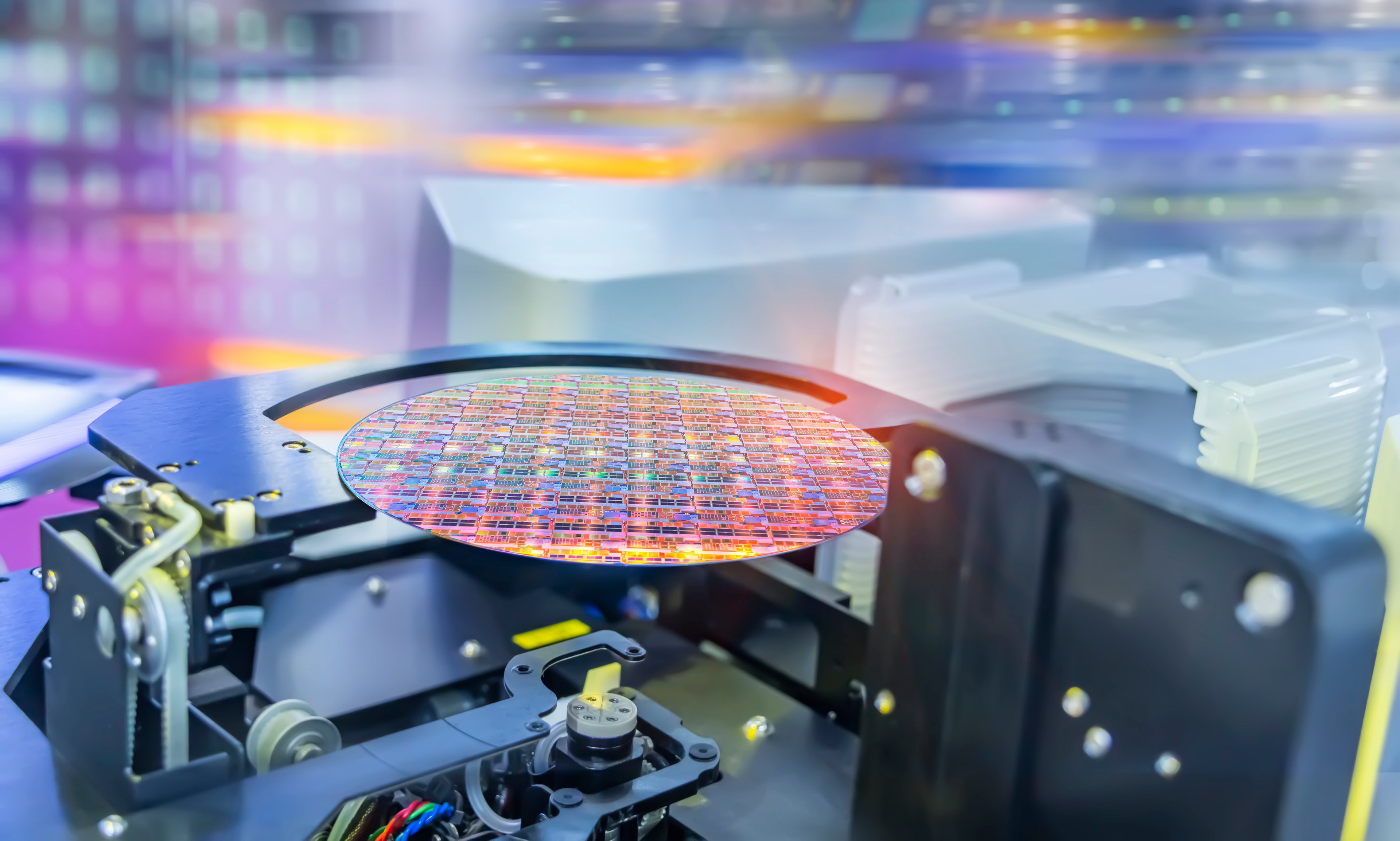
There has been a lot of talk in the investment community regarding the transistor density of Intel(INTC 4.64%) 14-nanometer technology. Intel says its 14-nanometer technology is inherently denser -- that is, more transistors can be packed into a given area -- than competing 14/16-nanometer technologies.
Interestingly though, Intel released some transistor counts and die areas of a couple of its 14-nanometer chips -- namely the 2+2 and 2+3 configurations of its Broadwell-U processors for low-power notebooks. The densities of these chips were about twice those of the 22-nanometer Haswell-U processors, but they were not as dense as, say, the Apple A8X built on Taiwan Semiconductor's 20-nanometer process.
It is well known that the density of a chip depends on the design goals for said chip. For example, at the Intel Developer Forum last year, Intel process technology guru Mark Bohr shared the following slide:

Source: Intel
The purpose of this slide was to illustrate that chip designers could use different interconnect stacks -- which play a key role in determining the performance and density of a chip -- to optimize for different things such as cost, density, and/or performance.
A real-world example
I would like to provide a "real-world" example of what Intel talked about in the slide. In particular, I would like to compare the densities of two products, both built on Intel 14-nanometer technology with vastly different transistor densities.
According to Intel, the Broadwell-U 2+3 configuration features 1.9 billion transistors and fits into an area of 133 square millimeters. This implies a density of approximately 14.3 million transistors per millimeter squared.
Now, take the recently released Intel Xeon D -- a highly integrated system-on-chip aimed at low-power servers. SemiAccurate reported that the Xeon D die weighs in at 160 square millimeters. Intel, in a recent post on Twitter, said its Xeon D processor is made up of 4.3 billion transistors -- implying a transistor density of approximately 26.88 million transistors per square millimeter.
That is nearly twice the density observed in the aforementioned Broadwell-U processor.
What is going on here?
If we work under the assumption that the transistor counts in both chips are apples to apples, then the question is: What is going on?
One thing to keep in mind is that Xeon D features eight CPU cores, 24 PCI Express lanes, and two integrated 10-gigabit Ethernet connections. That main complex also features 8 megabytes of L3 cache. The chip does not feature integrated graphics.
The CPU cores run at a base clock of 2.00GHz and can turbo up to a maximum of 2.6GHz, while the Broadwell CPU cores can turbo to up to 3.4GHz -- a 30% difference.
My guess: More of the Xeon D die is made up of cache memory, which is known to be denser than logic, helping chip density. Intel may also be using high density.
Furthermore, I suspect that the Xeon D is built using a metal stack optimized for density rather than for high frequencies (hence the max turbo of just 2.6GHz) to be able to integrate as much as possible into a relatively small footprint.
I would bet you Cherry Trail is even denser
Intel has not released the transistor count for its low-power 14-nanometer Atom processor known as Cherry Trail. This is probably the closest we would be able to get to an apples-to-apples comparison with a system-on-a-chip such as the Apple A8.
Given Intel's reluctance to talk about die sizes and transistor counts with respect to its Atom processors, I am not going to hold my breath for more detailed disclosures.