What happened
Shares of semiconductor equipment company Applied Materials (AMAT +3.84%) were rallying today, rising just over 5% at their morning highs.
The stock gained much more than its semiconductor equipment peers, which can be attributed to an exciting new product announcement this morning -- one that could enable Applied to take even more market share from competitors.

NASDAQ: AMAT
Key Data Points
So what
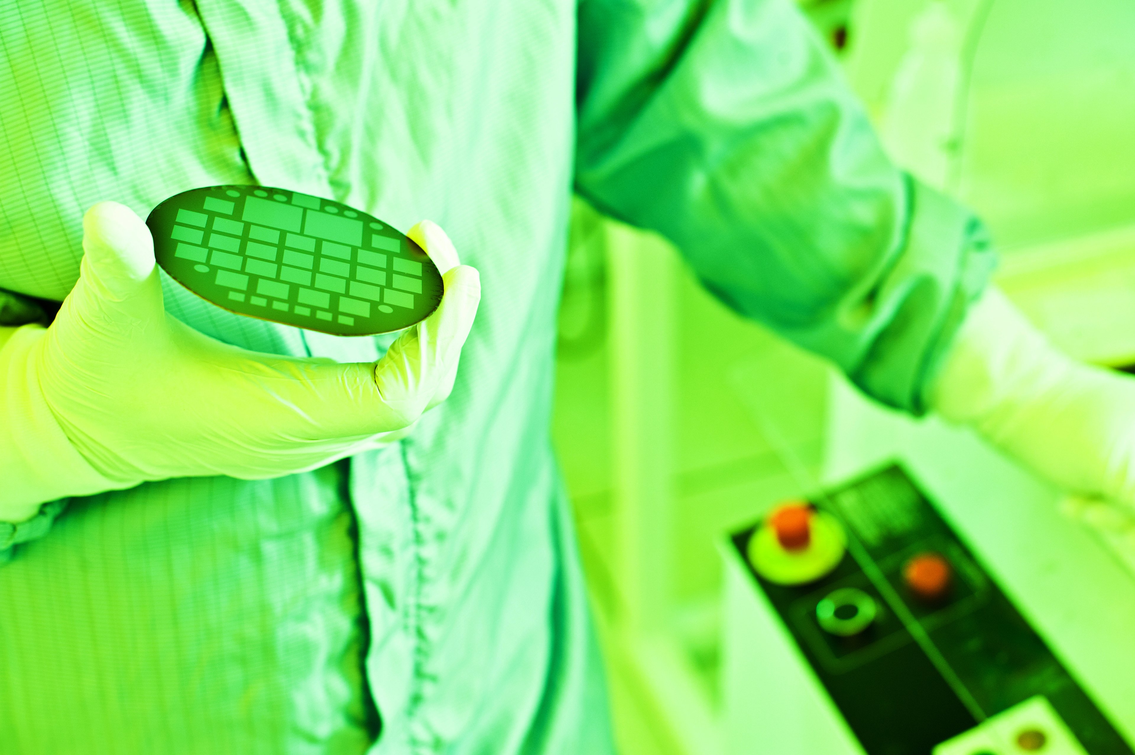
This morning, Applied Materials introduced two brand-new machines. That happens somewhat often; however, what was really exciting about today's announcement was that one of the product introductions was an entirely new kind of semiconductor equipment machine.
The new "pattern-stretching" machine has the potential to greatly lower the process steps needed for advanced leading-edge semiconductor production, thereby reducing costs and enabling the continued scaling of chips. That's a big deal.
It's called the Centura Sculpta, and it's an entirely new type of machine dedicated to "pattern-shaping" light patterns of advanced lithography. While the science is a bit complex, the main point is that advanced leading-edge nodes often require double patterning, or putting a wafer through two extreme ultraviolet process steps, in order to make smaller, more complex patterns than even extreme ultraviolet (EUV) light can print on a wafer.
However, Applied's Sculpta machine allows chipmakers to "stretch" or elongate and manipulate the EUV light pattern very precisely, shrinking the space in between different transistor patterns. That allows chipmakers to produce the most advanced chips now in just one EUV step, saving an entire process run containing even more lithography, etch, deposition, and metrology machines.
Applied believes the new machine will save foundries about $250 million per 100,000 wafer starts per month on capital costs, or $50 per wafer, while also greatly lowering electricity and water usage, lowering the carbon intensity of chipmaking.
In the press release, quotes from both Intel and Samsung revealed these two leading-edge foundries will be using pattern-shaping with Sculpta in their latest processes. One would imagine that if the new machine is successful, all other foundries would follow suit.
In addition, Applied also unveiled its new metrology system today, called the VeritySEM 10. Metrology is a known, crucial technology in all chipmaking, especially advanced chipmaking, but this new updated system is targeted at the highest-complexity, leading-edge layers.
Therefore, it's no surprise to see it introduced along with Sculpta in a compelling package for leading-edge chipmakers. The new system is designed to take sub-nanometer measurements specifically at the EUV layering step. The new machine is also geared for High-NA EUV, which is the latest and most advanced type of EUV machine, with even narrower light patterns that are even more difficult to measure and track.
Now what
I recently wrote about how Applied Materials' diverse machine lineup allows it to put R&D resources behind the highest-growth areas and toward solving chipmakers' most difficult problems. And while that diversity has enabled Applied to grow nicely on high-growth trailing-edge machines, bolstering results in the current year, management also said it expects to take market share on the high end as well, especially as chipmakers transition to gate-all-around (GAA) transistors.
We didn't have to wait long to hear how and why Applied will take share on advanced nodes. The new pattern-stretching Sculpta machine should not only bring in more revenue and profit to Applied -- it may even impede the growth of other equipment makers in EUV lithography and metrology, which could see some reduced usage as some steps are cut out of the chipmaking process.
All in all, Applied's announcement today only furthers the case for making the company a core semiconductor holding in investor portfolios.