Chip-giant Intel (INTC 1.80%) is dead set on reclaiming its manufacturing edge over foundry leader TSMC. The company's manufacturing roadmap includes launching five nodes in a four-year span.
Intel's Meteor Lake PC chips, set to launch this year, will use the Intel 4 process, the second process node in the plan. The final node, called Intel 18A, should be ready by the end of 2024. Intel expects this sub-2nm process to leapfrog TSMC.
The Intel 18A process should give Intel an edge in the PC and server-chip markets but will also mark an inflection point for Intel's foundry business. Companies that design chips that benefit from the most advanced manufacturing process -- think high-end smartphone system on a chip (SoCs) and artificial intelligence (AI) accelerators -- will have a viable option beyond TSMC.

NASDAQ: INTC
Key Data Points
Investing in packaging
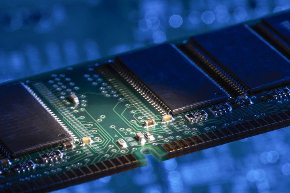
Manufacturing is only part of the equation. Once a semiconductor chip is fabricated, it must be packaged to protect it from the elements and enable connections to the outside world.
Old-school packaging methods are still widely used today and will continue to be used for the foreseeable future. These include wire bonding, which uses fine wire to connect a chip to a circuit board.
Advanced packaging techniques first emerged two decades ago and are now becoming increasingly important as chips become more complex. In advanced packaging, electrical connections are made at the wafer level, enabling better thermal characteristics and smaller package sizes.
AI chips, in particular, are driving demand for advanced packaging. Nvidia's A100 and H100 GPUs, which are widely used for AI training workloads, are packaged using TSMC's advanced chip-on-wafer-on-substrate packaging technology. Demand is so high that TSMC is rapidly expanding its advanced packaging capacity.
Intel is also investing in expanding its own advanced packaging capacity. Its 3D Foveros packaging technology, which is its take on 3D stacking, will be used for its upcoming Meteor Lake chips. With Meteor Lake, Intel is moving to a "chiplet" architecture that will allow multiple chips manufactured on different processes to be packaged together.
Beyond its own products, Intel will need to offer advanced packaging services to foundry customers. By 2025, the company is reportedly planning to quadruple its advanced chip packaging capacity, according to Nikkei Asia.
The plan includes building multiple new facilities in Malaysia. Notably, Amazon, Cisco, and the U.S. government have already committed to using Intel's advanced packaging technology.
The company reportedly will also offer advanced packaging services to customers, even if they don't manufacture their chips with Intel's foundry.
A foundry giant in the making
Come 2025, when the Intel 18A process is in production and Intel's advanced packaging capacity has been expanded, the company should be in a great position to win business from the most advanced chip designers.
Smartphone chips represent a major opportunity for Intel. The company and Arm are currently working together to optimize the Intel 18A process for Arm-based chips, and the company's advanced packaging investments will help it win business. Apple, for example, uses TSMC's advanced packaging services for many of its chips.
AI chips are another significant opportunity. If Intel can succeed in overtaking TSMC in terms of manufacturing technology while offering sufficient advanced packaging capacity, it will be in contention to manufacture AI chips from other companies, as well as its own.
The global foundry services market could reach $200 billion by 2028. With the manufacturing and advanced packaging investments Intel is making today, the company is positioning itself to scoop up a sizable chunk of a massive market in the long run.